


Search
440Hz.my - expanding musical horizons
Subscribe to our Feed


How to make high quality PCB at home
5 posters
Hi-Fi 4 Sale - Malaysia / Singapore Audio Forum & Marketplace | www.hifi4sale.net :: Discussion Forum & Knowledge Base :: DIY Projects
Page 1 of 1
![]()
 How to make high quality PCB at home
![]() by jat Thu Nov 15, 2012 8:16 pm
by jat Thu Nov 15, 2012 8:16 pm
How to make high quality PCB at home using UV exposure technique.
it's pretty easy for the avid diy-er to create a professional quality pcb at home with some simple steps. there's a lot of other guides available on the net on how to etch your own pcb at home, but usually tailored and written to parts available overseas which are hard to source at our local market.
so yeah, it's about time i share something that could benefit other people. i know it did to me. the move from breadboard to pcb is a godsend. i never had to trace the circuits back because of connection error during transfer from schematic onto circuit board.
to even attempt to create this kind of circuit on a breadboard are more or less, suicide.
first you need to draw the schematic and create a pcb board. i'm personally using diptrace. the free version are much more capable compared to eagle free version. and i personally think it's easier to use compared to eagle. diptrace also comes with the ability to import eagle's libraries so you'll have access to all of eagle's component libraries. anyway any pcb drawing program could be used as you please.
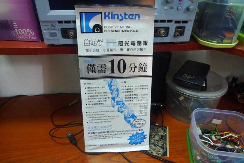
to create a pcb using uv exposure you need a pcb board with a uv reactive film. you could buy a uv film and attach it yourself (heard they could be ironed on) but i prefer these premade uv reactive pcb. quite readily available at your electronics shop. a lot of shops in jalan pasar stock these.
get the positive acting board. if you get the negative acting you need to print the pcb in negative print (later step). most shop usually sell the positive acting ones.
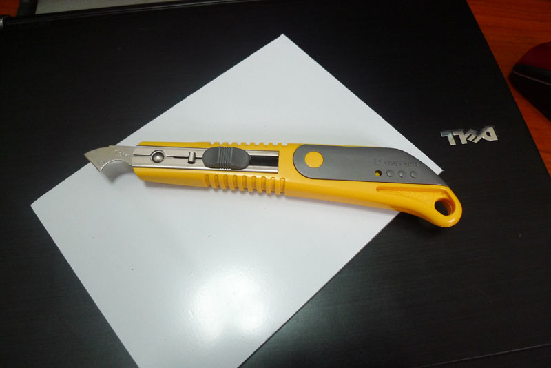
remove the board from the plastic and you'll see this grey film attached to one side of the board. cut the board to your required size. better to use these specialized plastic cutting knife and blade. it's soooo much easier and soooooo much safer. if you're wary about your fingers don't ever use a knife to cut your pcb. i've cut my thumb numerous times while doing so.
anyway if you absolutely must use a knife make sure to scrape/score/mark the line 20 times on both side to make a deep enough mark then snap them. if you use the plastic knife just 4-5 pass on both side and you could snap them much easier compared to using a knife. i really advice on the plastic knife as it's a lot safer. most large hardware store have them. just ask for a plastic knife/knife to cut acrylic or perspex or a knife with a blade that looks like a hook to cut plastics. usually around ~RM10 with spare blades selling for less than RM2 a piece.
it's pretty easy for the avid diy-er to create a professional quality pcb at home with some simple steps. there's a lot of other guides available on the net on how to etch your own pcb at home, but usually tailored and written to parts available overseas which are hard to source at our local market.
so yeah, it's about time i share something that could benefit other people. i know it did to me. the move from breadboard to pcb is a godsend. i never had to trace the circuits back because of connection error during transfer from schematic onto circuit board.
to even attempt to create this kind of circuit on a breadboard are more or less, suicide.
first you need to draw the schematic and create a pcb board. i'm personally using diptrace. the free version are much more capable compared to eagle free version. and i personally think it's easier to use compared to eagle. diptrace also comes with the ability to import eagle's libraries so you'll have access to all of eagle's component libraries. anyway any pcb drawing program could be used as you please.
to create a pcb using uv exposure you need a pcb board with a uv reactive film. you could buy a uv film and attach it yourself (heard they could be ironed on) but i prefer these premade uv reactive pcb. quite readily available at your electronics shop. a lot of shops in jalan pasar stock these.
get the positive acting board. if you get the negative acting you need to print the pcb in negative print (later step). most shop usually sell the positive acting ones.
remove the board from the plastic and you'll see this grey film attached to one side of the board. cut the board to your required size. better to use these specialized plastic cutting knife and blade. it's soooo much easier and soooooo much safer. if you're wary about your fingers don't ever use a knife to cut your pcb. i've cut my thumb numerous times while doing so.
anyway if you absolutely must use a knife make sure to scrape/score/mark the line 20 times on both side to make a deep enough mark then snap them. if you use the plastic knife just 4-5 pass on both side and you could snap them much easier compared to using a knife. i really advice on the plastic knife as it's a lot safer. most large hardware store have them. just ask for a plastic knife/knife to cut acrylic or perspex or a knife with a blade that looks like a hook to cut plastics. usually around ~RM10 with spare blades selling for less than RM2 a piece.

jat- Frequent Contributor

- Number of posts : 135
Age : 44
Location : malaysia
Registration date : 2009-03-15
Character sheet
Source(s):
Amplification:
Speakers:
![]()
![]()
Re: How to make high quality PCB at home
![]() by jat Thu Nov 15, 2012 8:35 pm
by jat Thu Nov 15, 2012 8:35 pm
i assume you already have a circuit that you wanna transfer to pcb. either downloaded from the net, some forum or drew from your own favorite program.
now to be useable for uv exposure, you need to print them onto something that will pass uv light through them. the ink or toner or the area printed with black will block the uv light but the material itself must let uv through them.
you could buy some specialty uv exposure transfer paper that looks like transparency paper. costs RM2~something a piece in A4 size. some electronic supplier stocks these. or, you could get TRACING PAPER. most stationery shop will have them in A4 and A3 size. quite easy to find. sold for less than RM1 a piece (A4 size).
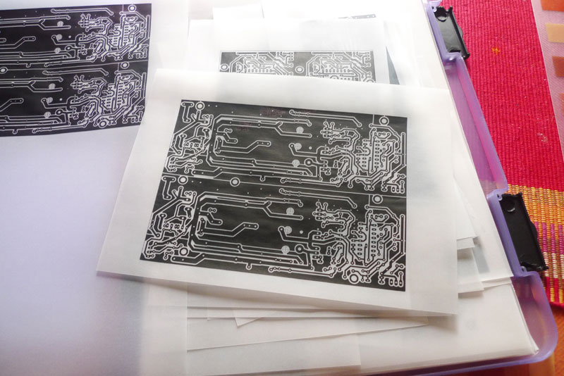
you can see that it's quite transparent, but not really clear as transparency paper. no matter as they pass UV light.
in my experience the paper weight (thickness) don't make much of a difference. it doesn't affect the exposure time. guides on the net advised to get the thickest that you could find, up to 100-120g. i've tried some 60g and currently using 80g.
i'm only using an inkjet to print them. have tried a laserjet but the blacks doesn't seem to be as dark as an inkjet. and since my inkjet does print as sharp as the laser, i just use the inkjet. you could have better result using laser but if you already have an inkjet (or a laserjet) at home, best to try them first before rushing to buy another printer.
now to be useable for uv exposure, you need to print them onto something that will pass uv light through them. the ink or toner or the area printed with black will block the uv light but the material itself must let uv through them.
you could buy some specialty uv exposure transfer paper that looks like transparency paper. costs RM2~something a piece in A4 size. some electronic supplier stocks these. or, you could get TRACING PAPER. most stationery shop will have them in A4 and A3 size. quite easy to find. sold for less than RM1 a piece (A4 size).
you can see that it's quite transparent, but not really clear as transparency paper. no matter as they pass UV light.
in my experience the paper weight (thickness) don't make much of a difference. it doesn't affect the exposure time. guides on the net advised to get the thickest that you could find, up to 100-120g. i've tried some 60g and currently using 80g.
i'm only using an inkjet to print them. have tried a laserjet but the blacks doesn't seem to be as dark as an inkjet. and since my inkjet does print as sharp as the laser, i just use the inkjet. you could have better result using laser but if you already have an inkjet (or a laserjet) at home, best to try them first before rushing to buy another printer.
jat- Frequent Contributor
- Number of posts : 135
Age : 44
Location : malaysia
Registration date : 2009-03-15
Character sheet
Source(s):
Amplification:
Speakers:
![]()
![]()
Re: How to make high quality PCB at home
![]() by jat Thu Nov 15, 2012 8:41 pm
by jat Thu Nov 15, 2012 8:41 pm
if you have some light area on the paper, or some place that you wanna make a correction or sign your own name  , use a sharpie marker or any permanent marker with oil based ink. these sharpies are cheap and sold by the dozen at tesco. and they come with an extra fine tip.
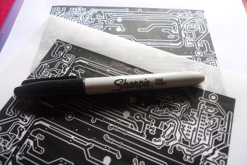
you could see the corrections that i've did to the pcb. there's some light area that i've corrected to make sure the uv is exposed evenly.
, use a sharpie marker or any permanent marker with oil based ink. these sharpies are cheap and sold by the dozen at tesco. and they come with an extra fine tip.you could see the corrections that i've did to the pcb. there's some light area that i've corrected to make sure the uv is exposed evenly.
jat- Frequent Contributor
- Number of posts : 135
Age : 44
Location : malaysia
Registration date : 2009-03-15
Character sheet
Source(s):
Amplification:
Speakers:
![]()
![]()
Re: How to make high quality PCB at home
![]() by jat Thu Nov 15, 2012 8:53 pm
by jat Thu Nov 15, 2012 8:53 pm
now remove the grey film that's attached to one side of the pcb that you've already cut. the uv film should look green or blue. never seen any other colour other than green and blue. anyway that's the uv reactive side.
and since it's reactive to uv, best to do all these inside a room, without any direct sunlight. you could turn on the light, but best to avoid sunlight. fluorescent light would still emit uv, but at very minute quantity that it (usually) won't affect the pcb. just don't put the pcb 30 cm away from a light source and you should be fine.
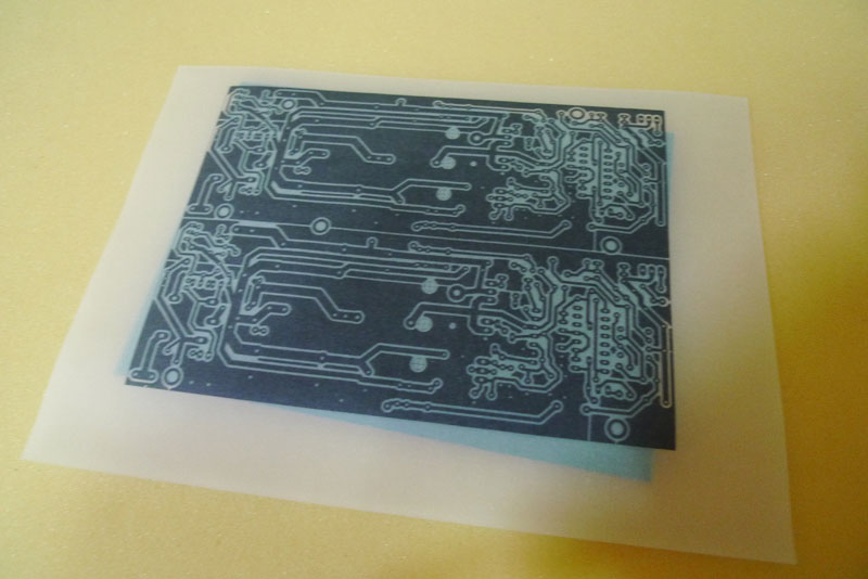
get the pcb that you've printed and would like to transfer and flip them. put the printed side (the side with the ink/toner on it) and stick it to the pcb. the ink/toner should be as close as possible to the uv film to avoid the traces from expanding during exposure.
i cut all my pcb to exact size but you could cut them a little bigger if you want. i personally never used a celltape to stick them to position. if you do just make sure not to overlap the celltape to parts of the pcb that you wanna remove. the celltape might block the uv light.
and since it's reactive to uv, best to do all these inside a room, without any direct sunlight. you could turn on the light, but best to avoid sunlight. fluorescent light would still emit uv, but at very minute quantity that it (usually) won't affect the pcb. just don't put the pcb 30 cm away from a light source and you should be fine.
get the pcb that you've printed and would like to transfer and flip them. put the printed side (the side with the ink/toner on it) and stick it to the pcb. the ink/toner should be as close as possible to the uv film to avoid the traces from expanding during exposure.
i cut all my pcb to exact size but you could cut them a little bigger if you want. i personally never used a celltape to stick them to position. if you do just make sure not to overlap the celltape to parts of the pcb that you wanna remove. the celltape might block the uv light.
jat- Frequent Contributor
- Number of posts : 135
Age : 44
Location : malaysia
Registration date : 2009-03-15
Character sheet
Source(s):
Amplification:
Speakers:
![]()
![]()

gloraglory- Frequent Contributor
- Number of posts : 106
Age : 50
Location : earth
Registration date : 2010-04-04
Character sheet
Source(s):
Amplification:
Speakers:
![]()
![]()
Re: How to make high quality PCB at home
![]() by jat Fri Nov 16, 2012 8:21 am
by jat Fri Nov 16, 2012 8:21 am
hopefully it'll benefit you like it did to me.gloraglory wrote:Like
anyway let's continue. the laptop ran out of battery last night.
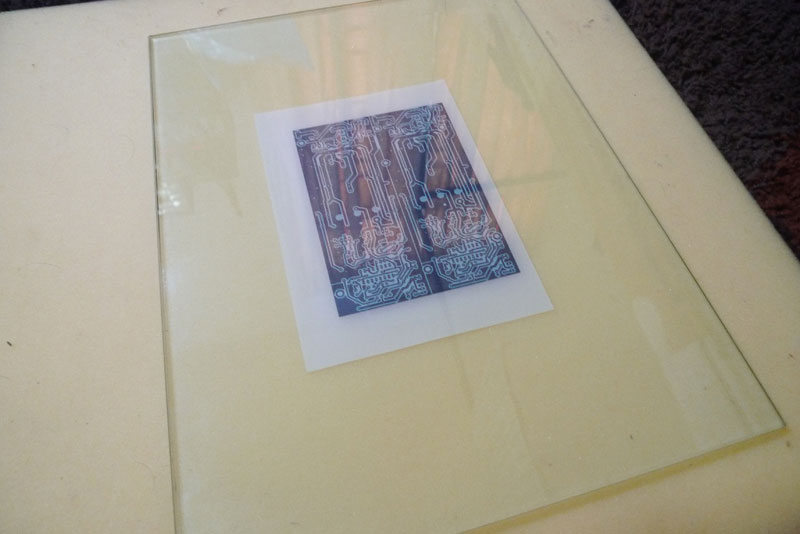
now sandwitch the pcb and paper with a sheet of glass. best to get a thick glass to put some weight to it. the glass will make sure the paper is nice and flat to the board.
some like to orientate the pcb and paper facing the bottom and expose the pcb from downside. that would also work, but it'll be harder to align the paper to the pcb since you can't see them. in which case you need to tape the paper to the pcb to avoid any movement.
i expose the pcb from the top so that i can make adjustment to the paper alignment and get exact exposure. i also put a flat sponge on the bottom to press the board. not an absolute necessity, but it helps. you can use some soft cloth, foam or any other soft material.
jat- Frequent Contributor
- Number of posts : 135
Age : 44
Location : malaysia
Registration date : 2009-03-15
Character sheet
Source(s):
Amplification:
Speakers:
![]()
![]()
Re: How to make high quality PCB at home
![]() by kp93300 Fri Nov 16, 2012 3:37 pm
by kp93300 Fri Nov 16, 2012 3:37 pm
Hi Jat,
Many thanks to you for putting up the thread . The tutorial is much appreciated .
kp93300
Many thanks to you for putting up the thread . The tutorial is much appreciated .
kp93300
kp93300- Regular

- Number of posts : 98
Age : 67
Location : kuching
Registration date : 2009-07-20
![]()
![]()
Re: How to make high quality PCB at home
![]() by jat Sat Nov 17, 2012 11:36 am
by jat Sat Nov 17, 2012 11:36 am
i forgot to add, do make sure there's no dust or any other small particle that's stuck in between the pcb board and paper. if there's dust there's a chance that it'll show after exposure.
now to the uv exposure.
now don't laugh. please?
hey i know it looks flimsy (and cheap), but it works. it looks flimsy (and cheap) because it is flimsy, and cheap.
you need to align the uv light source 5-10cm away from the pcb. nearer than 5 cm and you risk an uneven exposure. longer than 10cm and you risk not enough exposure.
if i remember correctly, rule of the thumb is that you need to double the exposure time for every 5 cm distance added.
i put the light source 5 cm away and found that 2 minutes of exposure time strikes the best balance for me. using different type of paper material, different weight, different kind of uv board, different printing method, different operating condition might require different exposure time. but most of the time it'll never be more than 5 minutes. best to try and experiment with your setup.
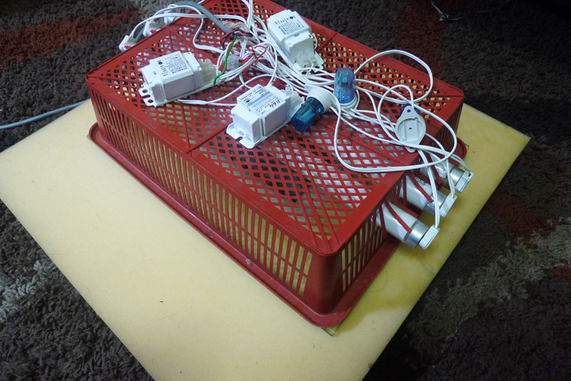
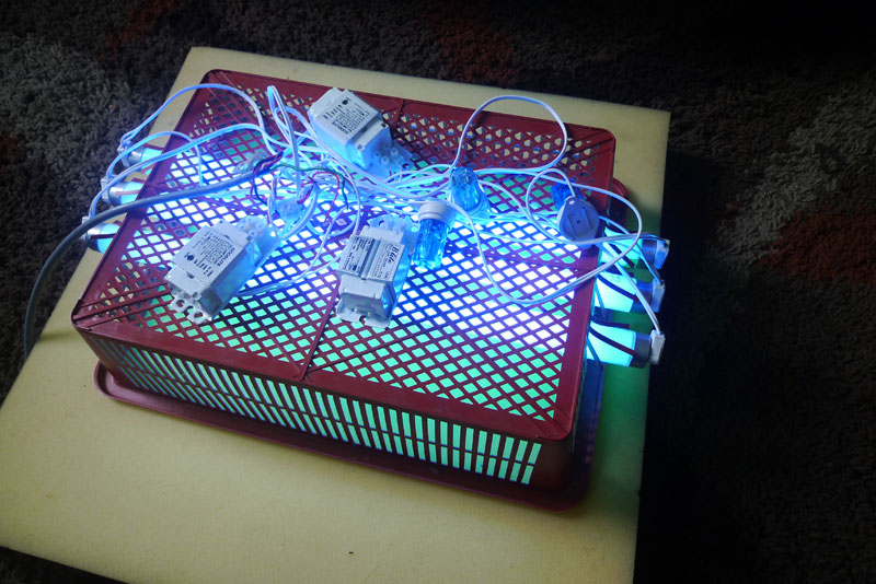
the uv light bulb that i'm using is 1.5 foot long 'black light'. these could be hard to find as not a lot of supplier stocks these. and you need to get a particular wavelength as there's quite a number of different wavelength uv light available on the market.
if i recall correctly there's 3 different wavelength uv light bulb on the market. there's the ones used to light bank notes and trace fake money. these types of uv light source usually comes with black/dark coloured bulbs. another one are those used in medical treatment. supposed to have the same wavelength as the uv of the sun. and those that can be used for our application, having the same wavelength as the uv light that are used to attract insects and electrocute them to death.
ala, the ones buzzing followed by a spark that you see in restaurants, canteens and food courts. they use the same wavelength and it's the bulb that you need to hunt. the bulb will look like an ordinary fluorescent light, white in colour and have contact poles on each side. they will emit a pale blue/pale purple light when powered on. ask for 'black light' or replacement bulb for insect killer. if you're handed a black coloured bulb then most probably it's not the correct one.
one of the bulb that i'm using even have the text 'black light' stamped next to the brand logo. sold for under RM20 a piece (1.5 foot long). there's also 1 foot and 2 foot long sold over here.
i've spaced the 3 bulbs 4.5 cm from each other to get a nice and even exposure for 15 cm pcb width. each bulb are wired like a normal fluorescent bulb with a ballast and a starter. there's no special wiring needed.
and since they work so good i kept skipping on making a proper case for them. hehe. total cost for the jig? probably less than RM100.
now to the uv exposure.
now don't laugh. please?
hey i know it looks flimsy (and cheap), but it works. it looks flimsy (and cheap) because it is flimsy, and cheap.
you need to align the uv light source 5-10cm away from the pcb. nearer than 5 cm and you risk an uneven exposure. longer than 10cm and you risk not enough exposure.
if i remember correctly, rule of the thumb is that you need to double the exposure time for every 5 cm distance added.
i put the light source 5 cm away and found that 2 minutes of exposure time strikes the best balance for me. using different type of paper material, different weight, different kind of uv board, different printing method, different operating condition might require different exposure time. but most of the time it'll never be more than 5 minutes. best to try and experiment with your setup.
the uv light bulb that i'm using is 1.5 foot long 'black light'. these could be hard to find as not a lot of supplier stocks these. and you need to get a particular wavelength as there's quite a number of different wavelength uv light available on the market.
if i recall correctly there's 3 different wavelength uv light bulb on the market. there's the ones used to light bank notes and trace fake money. these types of uv light source usually comes with black/dark coloured bulbs. another one are those used in medical treatment. supposed to have the same wavelength as the uv of the sun. and those that can be used for our application, having the same wavelength as the uv light that are used to attract insects and electrocute them to death.
ala, the ones buzzing followed by a spark that you see in restaurants, canteens and food courts. they use the same wavelength and it's the bulb that you need to hunt. the bulb will look like an ordinary fluorescent light, white in colour and have contact poles on each side. they will emit a pale blue/pale purple light when powered on. ask for 'black light' or replacement bulb for insect killer. if you're handed a black coloured bulb then most probably it's not the correct one.
one of the bulb that i'm using even have the text 'black light' stamped next to the brand logo. sold for under RM20 a piece (1.5 foot long). there's also 1 foot and 2 foot long sold over here.
i've spaced the 3 bulbs 4.5 cm from each other to get a nice and even exposure for 15 cm pcb width. each bulb are wired like a normal fluorescent bulb with a ballast and a starter. there's no special wiring needed.
and since they work so good i kept skipping on making a proper case for them. hehe. total cost for the jig? probably less than RM100.
thanks bro. i'll try and make it as detailed and as clear as possible. it will be lengthy (and seems complicated at first), but the results will be well worth it.kp93300 wrote:Hi Jat,
Many thanks to you for putting up the thread . The tutorial is much appreciated .
kp93300
jat- Frequent Contributor
- Number of posts : 135
Age : 44
Location : malaysia
Registration date : 2009-03-15
Character sheet
Source(s):
Amplification:
Speakers:
![]()
![]()
Re: How to make high quality PCB at home
![]() by jat Fri Nov 23, 2012 3:51 pm
by jat Fri Nov 23, 2012 3:51 pm
sorry for the delay in updating. got caught up with work.
this is how the tube light up. it's pale blue/pale purple. ish.
once you're satisfied with the placement of the pcb board and tracing paper turn on the light and wait for 2 minutes (or your time according to your setup).
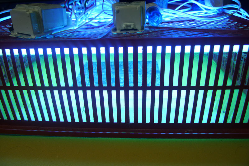
make sure to position the pcb board at the center of the light to get a nice and even light across the entire circuit.
this is how the tube light up. it's pale blue/pale purple. ish.
once you're satisfied with the placement of the pcb board and tracing paper turn on the light and wait for 2 minutes (or your time according to your setup).
make sure to position the pcb board at the center of the light to get a nice and even light across the entire circuit.
jat- Frequent Contributor
- Number of posts : 135
Age : 44
Location : malaysia
Registration date : 2009-03-15
Character sheet
Source(s):
Amplification:
Speakers:
![]()
![]()
Re: How to make high quality PCB at home
![]() by DrWho Fri Nov 23, 2012 4:37 pm
by DrWho Fri Nov 23, 2012 4:37 pm
Much appreciated jat! Many thanks.

DrWho- Frequent Contributor
- Number of posts : 376
Age : 71
Location : SS3 Petaling Jaya
Registration date : 2009-10-05
Character sheet
Source(s):
Amplification:
Speakers: Genelec
![]()
![]()
Re: How to make high quality PCB at home
![]() by jat Fri Nov 23, 2012 4:44 pm
by jat Fri Nov 23, 2012 4:44 pm
unlike toner transfer method where there's only one solution that's involved, this uv exposure require that the pcb be developed first before etching. some might argue that there's a couple of extra (unnecessary) steps involved (compared to the toner transfer method) and while i do agree with them, the extra steps are well worth it.
once the pcb have been exposed, remove it from the jig and dump them for a few minutes into a pcb developer.
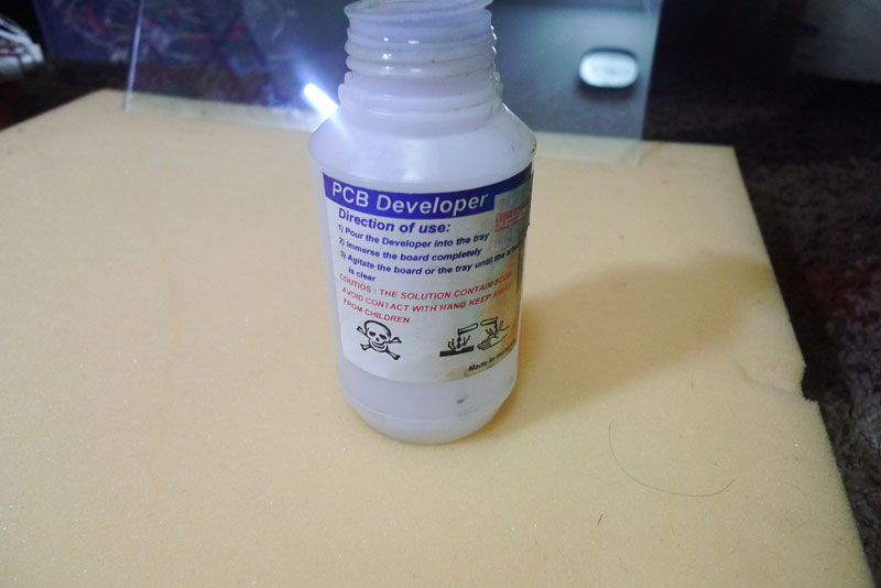
i'm using this premixed developer. there's also dry granules/powder that's available on the market. both will work, but you need to mix the granules first with some water before use. usually it's 1 packet to 500ml tap water.
the premixed cost me RM5 (or RM8 can't remember) for 250ml and the granules is a bit cheaper. i'm using a mixed of both since there's no granules selling over here. bought some from jalan pasar previously. been mixing them with each other without any fault.
there should be some faint image of the pcb transfer on the film. too faint to capture by my camera, but after exposure it should be there. the developer could be used a couple of time before losing their potency. i find that you could reuse them a lot more times by heating them a bit using hot water.
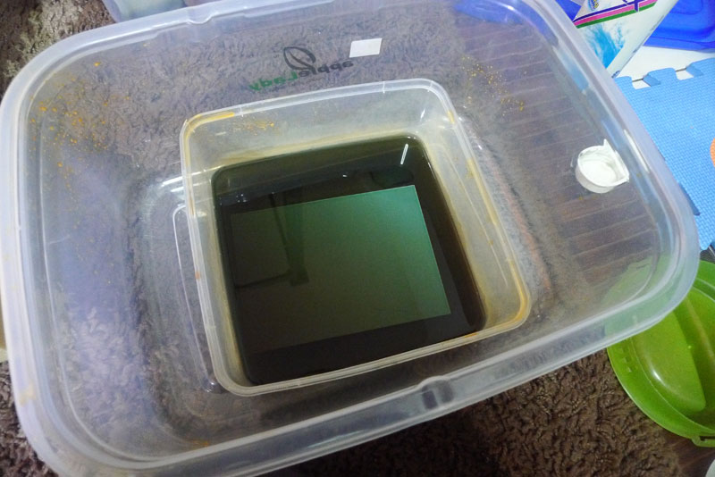
i use dual tray to use hot water to heat both the etching solution and developer solution. the larger tray is for the hot water and there's a couple of smaller tray according to the pcb size to avoid wastage as much as possible.
put the pcb board in the tray and pour some developer solution to the tray, soaking the pcb by a couple of millimeter. then agitate the developer to help with the process. the pcb traces should appear slowly.
read on the net that there's no downside in leaving the pcb in the solution for longer time than needed. i never leave them longer than needed. once all the non-traces area dissapear leaving only the traces nice and clear i remove them.
for my case it's usually around 30 seconds to a couple of minutes to get a nice and clear trace.
once the pcb have been exposed, remove it from the jig and dump them for a few minutes into a pcb developer.
i'm using this premixed developer. there's also dry granules/powder that's available on the market. both will work, but you need to mix the granules first with some water before use. usually it's 1 packet to 500ml tap water.
the premixed cost me RM5 (or RM8 can't remember) for 250ml and the granules is a bit cheaper. i'm using a mixed of both since there's no granules selling over here. bought some from jalan pasar previously. been mixing them with each other without any fault.
there should be some faint image of the pcb transfer on the film. too faint to capture by my camera, but after exposure it should be there. the developer could be used a couple of time before losing their potency. i find that you could reuse them a lot more times by heating them a bit using hot water.
i use dual tray to use hot water to heat both the etching solution and developer solution. the larger tray is for the hot water and there's a couple of smaller tray according to the pcb size to avoid wastage as much as possible.
put the pcb board in the tray and pour some developer solution to the tray, soaking the pcb by a couple of millimeter. then agitate the developer to help with the process. the pcb traces should appear slowly.
read on the net that there's no downside in leaving the pcb in the solution for longer time than needed. i never leave them longer than needed. once all the non-traces area dissapear leaving only the traces nice and clear i remove them.
for my case it's usually around 30 seconds to a couple of minutes to get a nice and clear trace.
jat- Frequent Contributor
- Number of posts : 135
Age : 44
Location : malaysia
Registration date : 2009-03-15
Character sheet
Source(s):
Amplification:
Speakers:
![]()
![]()
Re: How to make high quality PCB at home
![]() by jat Fri Nov 23, 2012 5:56 pm
by jat Fri Nov 23, 2012 5:56 pm
thanks bro. hopefully it'll help others in moving from breadboard & protoboard to proper pcb.DrWho wrote:Much appreciated jat! Many thanks.
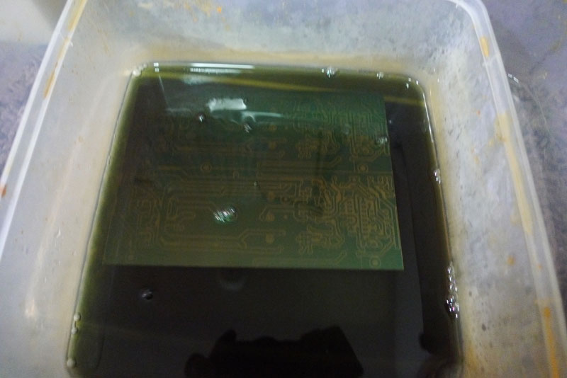
after removing the pcb board from the developer solution, wash them with tap water and use dishwashing liquid. you could use hand soap or shampoo but dishwashing soap would be best as they're quite thorough in removing the solution.
the developer solution (NaOH, natrium hidroksida, sodium hidroxide) is an alkaline and have corrosive properties. though i've never got into any trouble in handling the solution with my bare hands, it's probably best to wear gloves. wash immediately if you got them on your hands. don't want your hands to be like this now would we?
after washing them and drying them, you should arrive to something like this
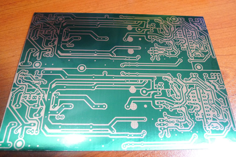
the traces and any copper pour should retain all of the film and the area to be removed will have the copper showing.
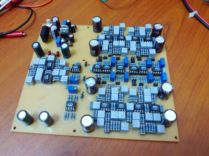
i've said high quality right?
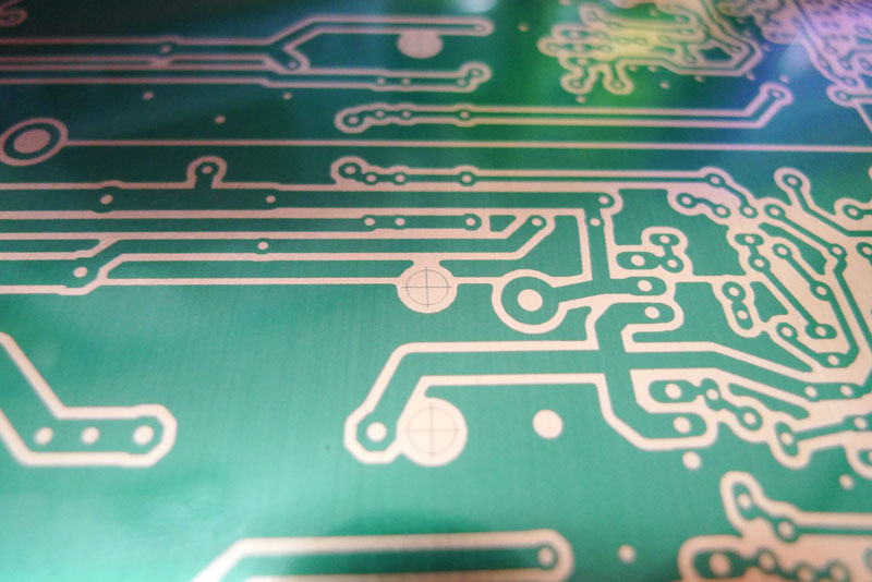
the lines are a fraction of a millimeter. even smaller than 0.1mm. as small as knife cut, i can't even measure it. and not just for this mounting hole. the lines are transferred perfectly for all the other 5 mounting holes that i have on the board.
and the same quality is repeatable over and over again. i get the same transfer quality with nearly all the boards that i've done, except for a few rare case. never had to throw away any board for a while now.
the ability to vary trace width by 0.1mm allow for better grounding scheme, which is helpful in large circuit with multiple ground points. this avoids ground loop or at least minimize the effect if should any still occur. the ability to have small signal traces also helps with minimizing EMI, RFI, reducing THD, etc.
jat- Frequent Contributor
- Number of posts : 135
Age : 44
Location : malaysia
Registration date : 2009-03-15
Character sheet
Source(s):
Amplification:
Speakers:
![]()
![]()
Re: How to make high quality PCB at home
![]() by shbehmal Sat Dec 07, 2013 9:41 am
by shbehmal Sat Dec 07, 2013 9:41 am
Thank You very much Jat for this valuable lesson.
shbehmal- Regular
- Number of posts : 63
Age : 57
Location : penang
Registration date : 2009-05-01
![]()
![]()
![]()

 Similar topics
» pioneer flagship home cinema amplifier (japan make) SOLD
» 2 Way high quality crossover
» High Quality Sealed CDs
» High quality rca cable 1.5M.
» WTB: high quality equipment rack
» 2 Way high quality crossover
» High Quality Sealed CDs
» High quality rca cable 1.5M.
» WTB: high quality equipment rack
Hi-Fi 4 Sale - Malaysia / Singapore Audio Forum & Marketplace | www.hifi4sale.net :: Discussion Forum & Knowledge Base :: DIY Projects
Page 1 of 1
Permissions in this forum:
You cannot reply to topics in this forum